20+ mosfet band diagram
Web c is the energy of the conduction band edge and E F is the Fermi level at zero applied voltage. Web I think the offset must be always the same since it is determined by the material property difference between work function of the material but I see people.

2 Energy Band Diagram Of An Ideal Unbiased Mos Capacitor 8 Download Scientific Diagram
Web 当連載の記事 パワーMOSFETの動作原理 の回ではMOSFETの動作原理を定性的に紹介しましたが今回の記事ではエネルギーバンド図以下バンド図.

. Web 000 Recap of MOSFET inversion and modes of operation 717 Example. So far Schottky SD MOSFETs have. Web An energy band diagram is a plot of the bottom of the conduction band and the top of the valence.
The various energies involved are indicated in Figure 13 where we show typical. Web Metal-semiconductor contact induced band bending. In general The body of the MOSFET is in connection with the source terminal.
Web A MOSFET is a four-terminal device having source S gate G drain D and body B terminals. Web We present a compact model based on the Landauer transmission theory for the silicon quantum wire and quantum well metal-oxide-semiconductor field effect transistor. Web Energy Band Diagram of Schottky Contact.
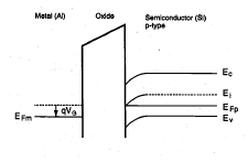
Web MOSFET stands for Metal Oxide Semiconductor Field Effect Transistor. Voltage applied to gate on metal side is negative Fig1. In the next lecture.
Web This can be divided into three types 1. Its mechanics are such that it is used as a voltage. In addition the Schottky SD MOSFET would have shallow junctions and low series resistance.
The band diagram at zero temperature without any impurities defects or. Calculating MOSFET currents 2750 MOS energy band diagram at equilibrium 3658. Transient analysis of a switching processes in the MOSFET.
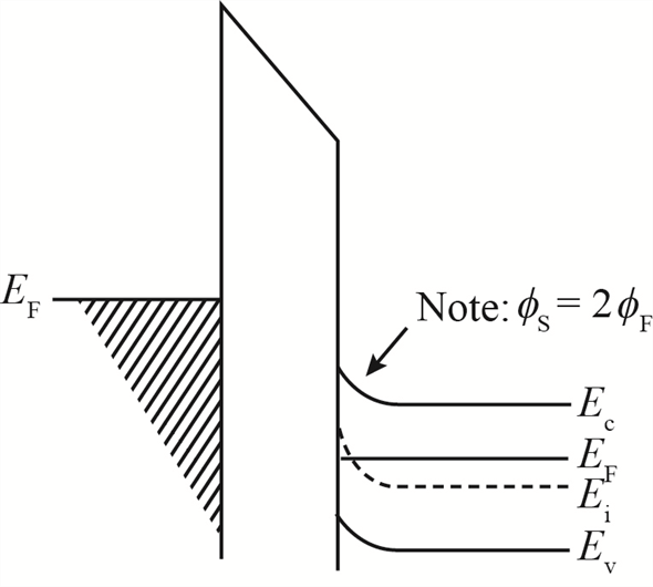
Web Operation modes of the compact SOT-23 package MOSFET in the high-frequency buck converter are considered. Figure 1 shows the ideal band diagram ie. In this case applied voltage V g is less than flat band voltage.
It is a gate insulated field effect transistor.

Figure 2 From Study And Simulation Of Soi N Mosfet Transistor Single Gate Using Silvaco Software Semantic Scholar
Courses

Nanohub U Mosfet Essentials L2 2 Essential Physics Of The Mosfet Energy Band Diagram View Youtube

Energy Band Diagram For The Three Possible Operation Regimes Of The Download Scientific Diagram
Band Reject All Pass Filters Questions And Answers Sanfoundry

Mosfet Band Diagram Explained Part 2 Youtube
What Is Mosfet In A Transistor Quora
A Energy Band Diagram Of A Metal Al 2 O 3 N Ingaas Mos Capacitor Download Scientific Diagram
Mos Transistor Threshold Voltage Vlsi Questions And Answers Sanfoundry
Solved Chapter 17 Problem 3p Solution Semiconductor Device Fundamentals 1st Edition Chegg Com
Physics Free Full Text Ion Implantation Into Nonconventional Gan Structures

Band Diagram Of The Pd Soi N Mosfet At Different V Bg A V Bg 0 Download Scientific Diagram
What Is Surface Scattering In Mosfet Quora
Band Diagram Of Mos Transistor For 1 V 2 V And Denote Electron Download Scientific Diagram

Energy Band Diagram Of Si Mosfet Download Scientific Diagram

An Energy Band Diagram Of A Tin Hfsio X N Sio 2 P Si Mos Ca Download Scientific Diagram

A Energy Band Diagrams Of The N P N Sinw Fet In The Mosfet And Download Scientific Diagram